
Materials whose electrical conductivity falls between conductors and insulators are called semiconductors. Atoms of group IV – A of periodic table are semiconductors.
Silicon is a semiconductor material. Atoms in pure silicon contain four electrons in outer orbit. In the crystal lattice structure of Si, the valence electrons of every Si atom are locked up in covalent bonds with the valence electrons of four neighboring Si atoms.
Intrinsic semiconductors:
In pure form, Si wafer does not contain any free charge carriers. Such types of pure semiconductors are called intrinsic semiconductors.
Extrinsic semiconductors:
In order to make useful semiconductor devices, materials such as phosphorus (P) and aluminium (Al) are added to Si. Those semiconductors that are doped with some specific impurities are called extrinsic semiconductors. These impurities modify the electrical properties of the semiconductor and make it more suitable for electronic conductivity. The extrinsic semiconductors are of two types; p-type and n-type.
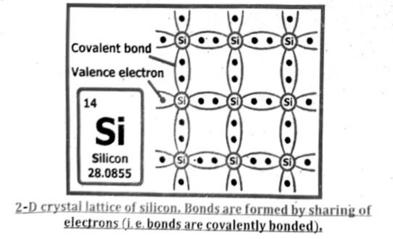
N-type and P-type semiconductors are both extrinsic semiconductors, meaning they are created by doping an intrinsic (pure) semiconductor with impurities. The key difference lies in the type of impurity used and the resulting charge carriers. N-type semiconductors have an excess of free electrons, making them negatively charged, while P-type semiconductors have an excess of “holes” (the absence of electrons, which behave like positive charges), making them positively charged.
N-type Semiconductors:
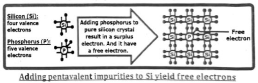
Doping: N-type semiconductors are created by doping an intrinsic semiconductor (like silicon or germanium) with a pentavalent element (one with five valence electrons), such as phosphorus, arsenic, or antimony.
Charge Carriers: The extra valence electron from the dopant atom is not needed for bonding and becomes a free electron, making the majority charge carriers in an N-type semiconductor.
Example: If you dope silicon (which has 4 valence electrons) with phosphorus (5 valence electrons), the extra electron from phosphorus becomes a free electron, making the material an N-type semiconductor.
Adding pentavalent impurities to Si yield free electrons
P-type Semiconductors:
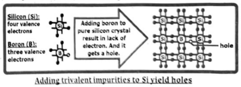
Doping: P-type semiconductors are created by doping an intrinsic semiconductor with a trivalent element (one with three valence electrons), such as boron, gallium, or indium.
Charge Carriers: The dopant atom creates a “hole” where an electron is missing, and this hole can move through the material as an electron from a neighboring atom fills the hole, leaving a new hole behind.
Example: If you dope silicon with boron (3 valence electrons), there's a missing electron (a hole) in the bonding structure.
Adding trivalent impurities to Si yield holes
Key Differences Summarized:
| Feature | N-type Semiconductor | P-type Semiconductor |
|---|---|---|
| Dopant Type | Pentavalent | Trivalent |
| Majority Charge Carriers | Electrons | Holes |
| Overall Charge | Neutral (dopant ions balance the charge of free carriers) | Neutral (dopant ions balance the charge of holes) |
| Fermi Level | Closer to the conduction band | Closer to the valence band |
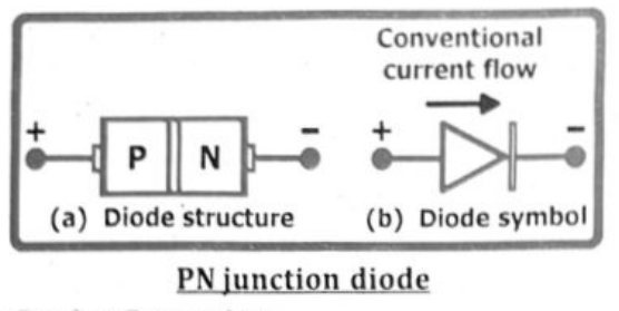
A diode is a two-terminal semiconductor device that acts like a one-way valve for electric current. It allows current to flow easily in one direction (forward bias) while significantly restricting or blocking current flow in the opposite direction (reverse bias). This unidirectional behavior is crucial for converting alternating current (AC) to direct current (DC), a process called rectification.
Key Concepts:
Anode and Cathode: Diodes have two terminals: an anode (positive) and a cathode (negative).
Forward Bias: When a positive voltage is applied to the anode and a negative voltage to the cathode, the diode is forward-biased, and current can flow easily.
Reverse Bias: When the voltage polarity is reversed, with the positive voltage applied to the cathode and negative to the anode, the diode is reverse-biased. In this state, the diode acts as an insulator, blocking current flow.
P-N Junction: Most diodes are made of a p-n junction, where a p-type semiconductor (with “holes” as majority carriers) is joined to an n-type semiconductor (with electrons as majority carriers).
Depletion Region: When the p-n junction is formed, a depletion region forms near the junction. This region has few free charge carriers and acts as a barrier to current flow.
How it Works:
Forward Bias: Under forward bias, the applied voltage reduces the width of the depletion region. This allows current to flow through the diode as electrons and holes move across the junction.
Reverse Bias: In reverse bias, the depletion region widens, effectively preventing current flow.
Threshold Voltage: Diodes typically require a certain threshold voltage (e.g., 0.7 V for silicon diodes) to start conducting in the forward direction. Below this voltage, they remain in a high-resistance state.
Applications:
Rectification: Diodes are fundamental components in power supplies, converting AC voltage to DC voltage.
Signal Processing: They are used in radio receivers to demodulate signals and extract information from modulated radio waves.
Voltage Regulation: Diodes can be used to regulate voltage levels in circuits.
Switching: Diodes can act as electronic switches, controlling the flow of current based on voltage conditions.
Protection Circuits: They can protect circuits from voltage spikes or reverse voltage.
A PN junction is the interface formed when a p-type semiconductor (with an excess of holes) is joined with an n-type semiconductor (with an excess of electrons).
The formation of the depletion region arises from the diffusion of charge carriers across this junction. Excess electrons from the n-type side diffuse to the p-type side, and excess holes from the p-type side diffuse to the n-type side.
This diffusion process leaves behind exposed, ionized dopant atoms (positive ions on the n-side and negative ions on the p-side) near the junction, creating a region devoid of free charge carriers, the depletion region.
Detailed explanation:
Formation of the PN Junction:
A p-type semiconductor has an excess of holes (vacant electron positions), while an n-type semiconductor has an excess of free electrons.
When these two materials are joined, a PN junction is formed.
Diffusion of Charge Carriers:
Due to the concentration gradient, free electrons from the n-type side diffuse to the p-type side, and holes from the p-type side diffuse to the n-type side.
This diffusion process is driven by the tendency of particles to move from areas of high concentration to areas of low concentration.
Depletion Region Formation:
As electrons move from the n-type to the p-type, they leave behind positively charged donor ions (impurities) that were originally present in the n-type material.
Similarly, as holes move from the p-type to the n-type, they leave behind negatively charged acceptor ions (impurities) that were originally present in the p-type material.
These immobile, ionized dopant atoms create a region near the junction that is depleted of free charge carriers (electrons and holes).
This region is called the depletion region or depletion layer.
Electric Field and Potential Barrier:
The depletion region is characterized by an electric field, pointing from the positive ions (on the n-side) to the negative ions (on the p-side).
This electric field creates a potential barrier that opposes the further diffusion of charge carriers across the junction.
The potential barrier prevents the free flow of electrons and holes across the junction under normal conditions.
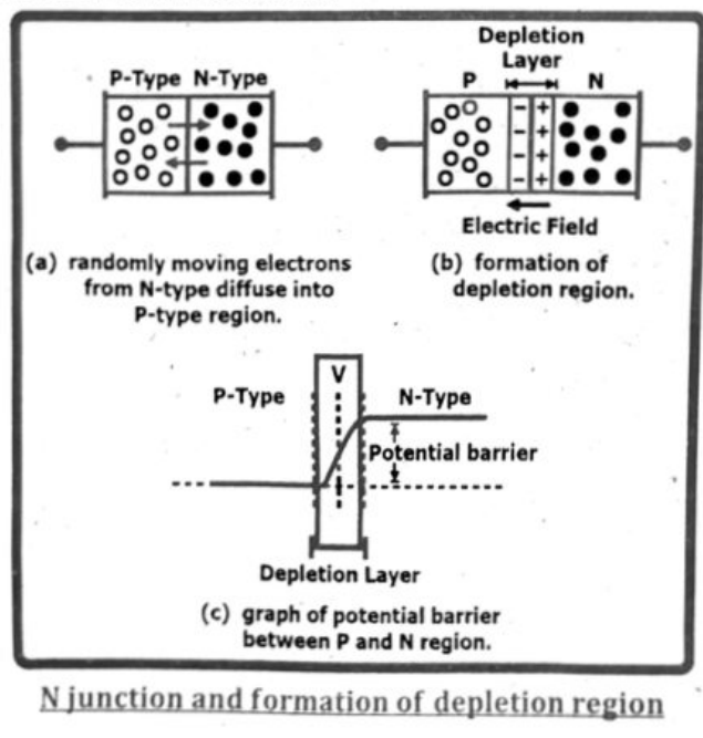
In essence, the diffusion of charge carriers across the PN junction creates a region depleted of free carriers and establishes an electric field that opposes further diffusion, resulting in the formation of the depletion region and the potential barrier.
Under-biasing a diode, whether forward or reverse, means not applying enough voltage to cause significant current flow. In forward bias, a small voltage, typically below the diode’s threshold voltage, results in minimal current flow. In reverse bias, applying a voltage below the breakdown voltage leads to a very small leakage current.
Forward Under-biasing:
Low current flow: A forward-biased diode only starts conducting when the forward voltage exceeds a certain threshold voltage (around 0.7 V for silicon and 0.3 V for germanium). Below this voltage, the current flow is minimal.
Depletion region still present: The depletion region, which is a region devoid of free charge carriers at the p-n junction, is still present, although it’s narrower than in reverse bias.
High resistance: The diode offers high resistance to current flow in this region, acting as a “nearly” open circuit.
Example: Applying a forward voltage of 0.2 V to a silicon diode would result in a very small forward current, as the applied voltage is below the typical 0.7 V threshold.
Figure: Forward bias
Reverse Under-biasing:
Minimal leakage current: When a diode is reverse-biased, a small reverse current (leakage current) flows due to minority carriers. This current is typically very small and is dependent on temperature and the diode material.
Depletion region widens: The depletion region at the p-n junction widens significantly.
High resistance: The diode presents a very high resistance to current flow, effectively blocking current in the reverse direction.
Example: Applying a reverse voltage of - 5 V to a silicon diode would result in a small leakage current, much smaller than the forward current that would flow under forward bias.
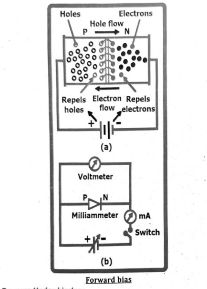
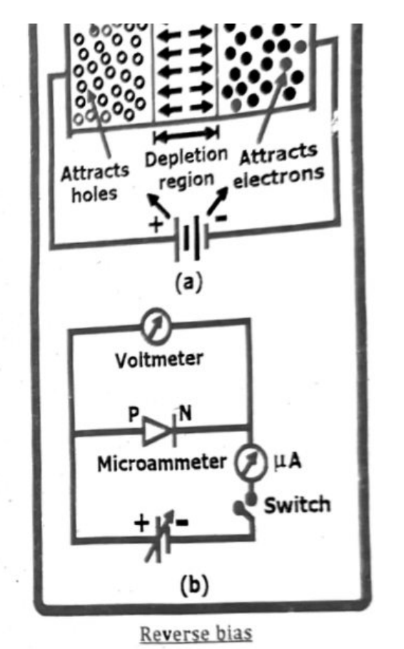
In semiconductor diodes, both electrons and holes contribute to current flow, but their roles differ based on the diode's type and bias. In forward bias, electrons move from the n-type region to the p-type region, while holes move from the p-type region to the n-type region, resulting in current flow. In reverse bias, a depletion region forms, hindering the flow of both electrons and holes and thus minimizing current.
Detailed explanation:
Forward Bias:
- When a positive voltage is applied to the p-type side and a negative voltage to the n-type side (forward bias), the barrier potential at the junction is reduced.
- Electrons in the n-type material are pushed towards the junction, and holes in the p-type material are also pushed towards the junction.
- These majority carriers (electrons in n-type and holes in p-type) then cross the junction and recombine, leading to current flow.
- The current is carried by the movement of both electrons and holes in opposite directions, but their combined effect results in a conventional current flow in the same direction.
Reverse Bias:
- When a negative voltage is applied to the p-type side and a positive voltage to the n-type side (reverse bias), the barrier potential at the junction is increased.
- This increase in barrier potential repels both electrons and holes away from the junction.
- A depletion region (a region with a lack of charge carriers) forms near the junction, hindering the flow of both electrons and holes.
- However, a small reverse current can still flow due to minority carriers (electrons in p-type and holes in n-type) that are thermally generated and can cross the junction.
Doping and Carrier Concentration:
- Semiconductors are doped to increase their conductivity. N-type semiconductors have an excess of electrons (majority carriers), while P-type semiconductors have an excess of holes (majority carriers).
- This doping significantly impacts the behavior of diodes and other semiconductor devices.
- In N-type material, electrons are the majority carriers, and holes are the minority carriers. In P-type material, holes are the majority carriers, and electrons are the minority carriers.
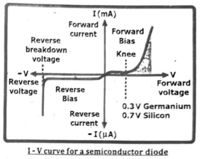
A diode is a semiconducting device which only allows current to flow through it in one direction. This can be seen in the I-V curve. At positive voltages, the curve rises exponentially, indicating that current is free to flow through the device. At negative voltages, the current remains nearly at zero.
The current (I) verses voltage (V) graph for a pn junction is shown in figure. It can be seen that, in the forward bias region, current and voltage are positive. When the forward voltage is less than ‘Vd’, the forward current is nearly zero so the diode does not conduct. When the forward current is equal to ‘Vd’, the diode starts to conduct.
In the reverse bias region, current and voltage are negative. As reverse bias voltage is raised, the depletion region width increases and a point comes when the junction breaks down. This results in large flow of current.
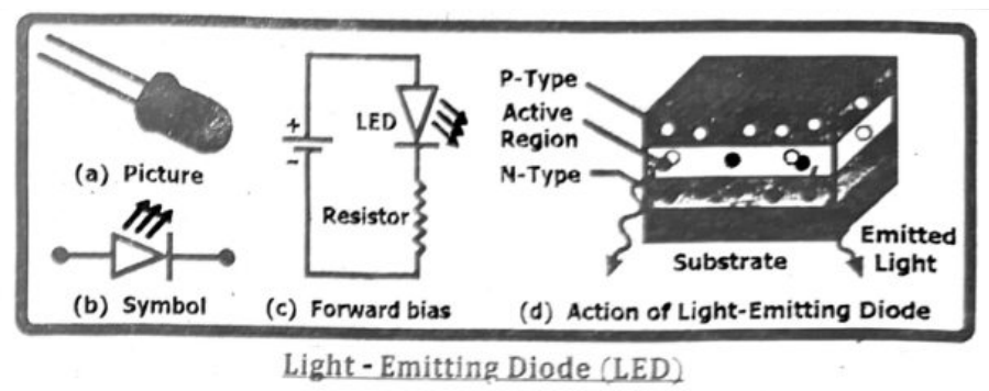
A light-emitting diode (LED) allows current to flow in one direction (forward bias) and emits light when current passes through it. This occurs because of the unique semiconductor material used in its construction, which allows electrons to recombine with electron holes, releasing energy in the form of photons (light).
Here’s a more detailed explanation:
One-Way Current Flow (Diode Action):
LEDs, like other diodes, are made of a semiconductor material that is specifically doped to create a p-n junction.
This junction allows current to flow easily in one direction (forward bias) and blocks current flow in the opposite direction (reverse bias).
In forward bias, the positive side of the circuit (anode) is connected to the p-type material, and the negative side (cathode) is connected to the n-type material.
This allows electrons to flow from the n-type material to the p-type material, where they combine with “holes” (the absence of electrons).
Light Emission (Recombination):
When an electron recombines with a hole in the semiconductor material, it releases energy in the form of a photon, which is a particle of light.
The specific semiconductor material and doping used in the LED determine the wavelength (and thus the color) of the emitted light.
For example, different materials like gallium arsenide phosphide or indium gallium nitride are used to produce red, green, and blue light, respectively.
In summary, LEDs utilize the unique properties of semiconductor materials to allow current to flow in one direction and, when forward biased, to emit light as electrons recombine with holes and release photons.
Light-Emitting Diode emits energy in the form light and hence they glow when the electric current passes through it. These diodes are made from gallium arsenide phosphide (GaAsP) and gallium phosphide (GaP).
A light-emitting diode (LED) is a semiconductor device that emits light when an electric current passes through it. This occurs when electrons recombine with electron holes in the semiconductor material, releasing energy in the form of photons.
The color of the emitted light depends on the energy band gap of the semiconductor material. LEDs are widely used in various applications due to their energy efficiency, long lifespan, and durability.
Working Principle:
P-N Junction: An LED is essentially a diode, specifically a forward-biased p-n junction.
Electron-Hole Recombination: When a forward voltage is applied, electrons from the n-type material and holes from the p-type material move towards the junction.
Photon Emission: At the junction, these electrons and holes recombine, releasing energy in the form of photons, which is the light we see.
Color Determination: The energy of the emitted photons, and thus the color of the light, is determined by the band gap of the semiconductor material.
Applications:
LEDs are used in a vast array of applications, including:
Lighting: Household lighting, streetlights, automotive lighting.
Displays: Television screens, computer monitors, mobile phones.
Signage: Traffic lights, billboards, decorative lights.
Electronics: Indicator lights, backlighting.
Medical: Surgical lighting, diagnostic equipment.
Horticulture: LED grow lights for plants.
Relays and switching circuit:
Relays are switches that open and close circuits electromechanically or electronically. Relays control one electrical circuit by opening and closing contacts in another circuit.
How Does a Relay Work?
Relays function using electromagnetic induction. To operate the relay, the coil surrounding the relay's core is energized by electricity from the power source controlling it. As the relay is energized, it creates a magnetic field that attracts the contact and completes the circuit within the relay. This turns on or off the load being controlled.
The primary purpose of a relay is to protect the electrical system from too high of a voltage or current, allowing the safe operation of any equipment it connects to.
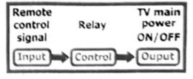
A Relay is an electrically operated switch that open and close the circuits by receiving electrical signals from outside sources. It consists of a set of input terminals for a signal and a set of operating contact terminals. For example consider figure, when you push the button on a TV remote to watch TV, it sends an electrical signal to the relay inside the TV, turning the main power ON.
Relays are very important in electronics. These are used to control a high power or high voltage circuit (or devices) with a low power circuit. A relays embedded in electrical products receive an electrical signal and send the signal to other equipment by turning the switch ON and OFF. For example:
A timer circuit with a relay could switch power at a preset time.
Relays are used to protect electrical circuits from overload or faults.
Relays are used to turn on / off high-power devices like lamps or garage door motors with just a small DC voltage signal.
TYPES OF RELAY:
There are various types of relays used in many applications to control different amounts of currents and number of circuits.
Relay technology can be divided into two main categories:
Movable contacts (mechanical relay) and no movable contacts.
Movable Contacts (Mechanical Relay): This type of relay has contacts that are mechanically motivated to open / close by a magnetic force to switch signals, currents and voltages ON or OFF.
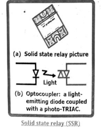
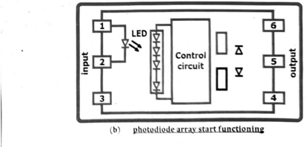
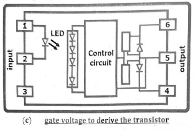
No Movable Contacts: Solid state relay (SSR), as shown in figure (a), is an example of No-movable contact. It does not have any moving part, thus increasing long-term reliability. A solid state relay uses semiconductor and electrical switching device, activated by the control signal, to switch the controlled load. An optocoupler (a light-emitting diode coupled with a photo transistor or photo-TRIAC) can be used to isolate control and controlled circuits, as shown in figure (b). Solid state relay (SSR) is commonly used for two reasons; a faster-switching process and durability.
Operating Principles of Solid State Relays:
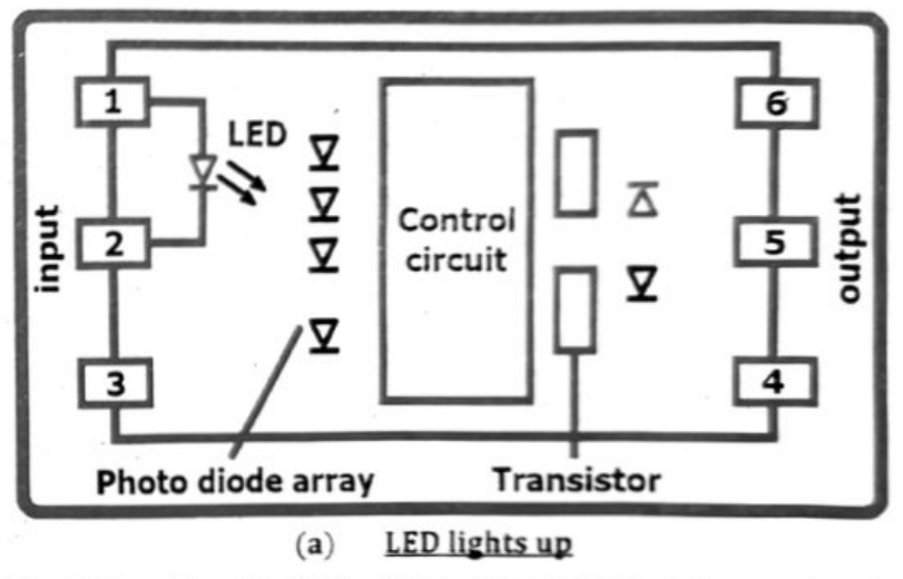
Solid state relays (SSRs) utilize electronic components to switch electrical loads, unlike electromechanical relays that use physical contacts. They operate by converting an input control signal into an optical signal, which then triggers a semiconductor switch (like a thyristor or MOSFET) to control the load current. This process provides isolation between the input and output circuits, enhancing safety and reducing electrical noise.
Solid State relays operate according to the following principles.
The LED lights up when the current is connected at the input side as shown in figure (a).
The light sent by the LED will be converted into voltage gain when it is received by the photodiode as shown in figure (b).
This voltage will be a gate voltage to derive the transistor via control circuit as shown in figure (c).
TRANSISTOR AS A SWITCH:
A transistor can function as a switch by utilizing its ability to control current flow between its collector and emitter terminals based on the current applied to its base. Specifically, NPN transistors act as switches by allowing current to flow from the collector to the emitter when a small base current is present, effectively turning the switch “on”. Conversely, when the base current is removed, the transistor turns “off”, blocking current flow.
The transistor can be used as a switch if biased in the saturation and cut-off regions. The collector C and emitter E of transistor behave as the terminal of switch. The base ‘B’ and emitter ‘E’ act as the control terminal to decide the state of the switch either on or off. The main reason behind using the transistor as a switch is that the current at the base (IB) controls the current present at the collector (IC): as from the relation IC = β IB. If the current at the base exceeds the minimum cut-off value, then the behavior of the transistor is like a closed switch otherwise it will behave like an open switch.
Suppose we have a lamp that we want to turn on and off with a switch, as shown in the figure.
Transistor as a switch
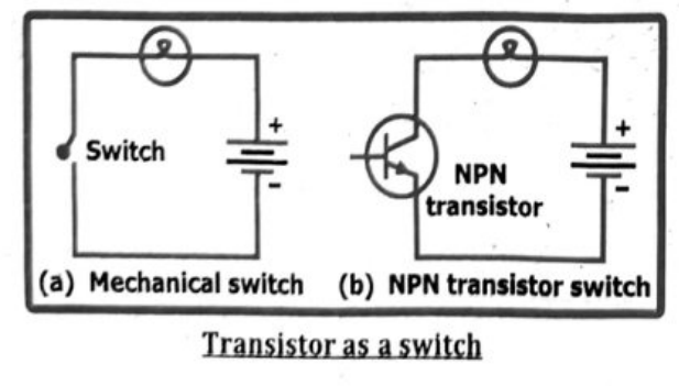
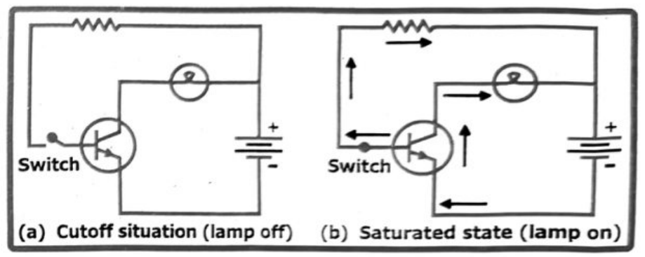
If the base of transistor is not connected to a suitable voltage, the base current will become zero. If the switch is open as shown in figure (a), there will be no current through the base. According to the relation $I_C = \beta I_B$, no current will flow from the collector to the emitter. In this situation, the resistance between C and E becomes infinite and CE behaves as an open switch. In this state, the transistor is said to be in cutoff.
If the switch is closed as shown in figure (b), current will be able to flow from the base to the emitter of the transistor through the switch. This base current will enable a much larger current flow from the collector
Electronic devices, like computers, are indeed built from digital logic circuits, which are essentially sophisticated networks of switches. These circuits use voltage levels to represent binary digits, with high voltage representing “1” and low voltage representing “0”. By combining these “switches” (logic gates) in various ways, complex operations can be performed.
Digital Logic Circuits: These circuits are designed to process information in a discrete, digital manner, using binary values (0 and 1).
Switches: The fundamental building blocks are often transistors, which act as electronic switches that can be turned “on” (allowing current to flow) or “off” (blocking current).
Voltage Levels: These switches are controlled by voltage levels. A high voltage (e.g., +5V) is often designated as “1”, while a low voltage (e.g., 0V) is designated as “0”.
Logic Gates: These are basic circuit components that implement logical operations (AND, OR, NOT, etc.) using these voltage-based binary signals.
Combining Logic Gates: By combining multiple logic gates, more complex circuits can be built, such as adders, registers, and even microprocessors. These complex circuits can perform various computations and control the behavior of the electronic device.
Example: A simple AND gate, for instance, would output a high voltage (1) only if both of its inputs are high (1).
By combining many logic gates, devices like calculators, computers, and smartphones can store data, make decisions, and perform tasks.
Boolean logic is the foundation of how computers convert analogue data into digital form. Analogue data can have any value, like the changing temperature or sound. But computers only understand digital data, that is, 0s and 1s. A bit (binary digit) is the smallest unit of data that a computer can process and store.
A bit is the smallest possible unit of data in a computer.
One bit holds a value of either 0 or 1.
A byte is a group of 8 bits, like 10001011 for example.
Each bit can be either 0 or 1, and with 8 bits in a byte, there are $2^8 = 256$ different values a byte can have.
Boolean logic uses rules (like AND, OR, NOT) to decide if a signal should be a 0 (off) or 1 (on). When analogue signals are measured, they are compared to certain levels, and Boolean logic helps decide which digital value (0 or 1) they should become.
So, Boolean logic helps turn real-world signals into digital signals that computers can process.
A bit is the smallest unit of digital information and can have a value of either 0 or 1. A byte, on the other hand, is a group of bits that is typically composed of eight bits. Bytes are used to represent larger amounts of information, such as letters, numbers, or symbols.
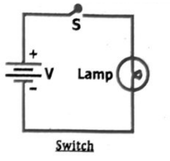
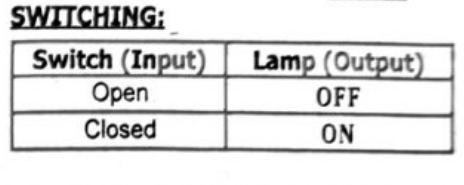
SWITCHING:
| Switch (Input) | Lamp (Output) |
|---|---|
| Open | OFF |
| Closed | ON |
LOGIC GATES:
Logic gate is an elementary building block of a digital circuit. Most logic gates have two inputs and one output. At any given moment, every terminal is in one of the two binary conditions low (0) or high (1), represented by different voltage levels. Thus, having the ability to perform a logical operation.
Truth table:
The table which shows all inputs & output possibilities for a logic circuit is termed as truth table. It is also known as the tables of combination of independent variables and dependent variables i.e. input to output.
Logic equation gives a relationship between input and output variables.
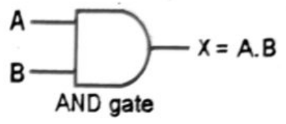
(i) AND GATE:
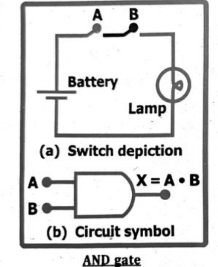
AND Gate is physical realization of the logical multiplication. It is the implement of AND operation.
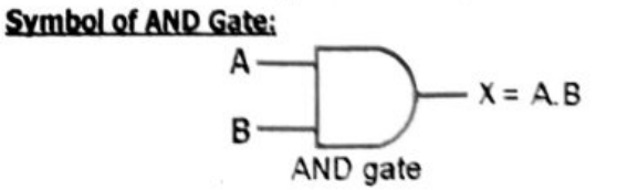
The logic equation for the AND function can simply be written as $X = A \cdot B$ (read as ‘X equals A AND B’).
Symbol of AND Gate:
Truth table of AND Gate:
| Switch (Input) | Lamp (Output) | |
|---|---|---|
| A | B | $X = A \cdot B$ |
| 0 | 0 | 0 |
| 1 | 0 | 0 |
| 0 | 1 | 0 |
| 1 | 1 | 1 |
Output of AND gate will be 1 only when all of its inputs are 1, and for all other situations output of AND gate will be ‘0’.
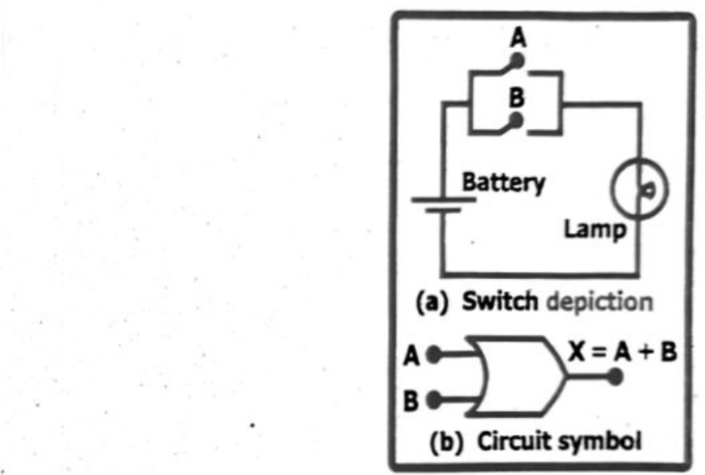
(ii) OR GATE:
OR Gate is physical realization of the logical addition. It is the implement of OR operation.
The logic equation for the OR function can simply be written as $X = A + B$ (read as “X equals A OR B”).
Symbol of OR Gate:
Output of OR gate will be ‘0’ only when all of its inputs are ‘0’, and for all other situations output of OR gate will be ‘1’.

Truth table of OR Gate:
| OR GATE | ||
|---|---|---|
| Switch (Input) | Lamp (Output) | |
| A | B | $X=A+B$ |
| 0 | 0 | 0 |
| 1 | 0 | 1 |
| 0 | 1 | 1 |
| 1 | 1 | 1 |
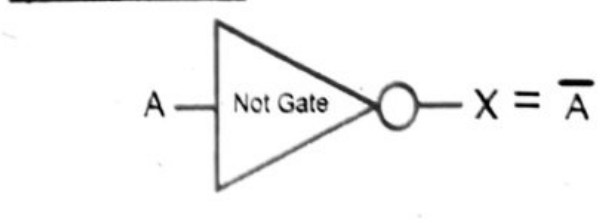
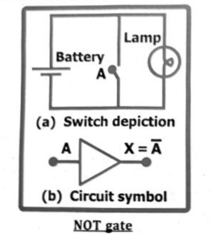
(iii) NOT GATE:
The electronic circuit which implements NOT operation is known as NOT gate.
NOT gate has one input and one output. If a High (1) input comes in, it produces a Low (0) output. If a Low (0) input comes in, it produces a High (1) output. This gate is also called an inverter as it inverts the input signal.
The Logic equation for an inverter is written $X=\overline{A}$ (and read as X equals NOT A). The symbol, its switch representation and truth table for the inverter gate are shown in figure below.
Symbol of NOT Gate:
Boolean expression for NOT operation is: $X=\overline{A}$ (read as “X equals A NOT”)
(iv) NAND GATE:
The combination of AND gate with NOT gate is called NAND gate.
A NAND gate as an AND gate with a NOT gate at its output. The symbol for a NAND gate is made from an AND gate with the inversion circle (bubble) at its output as shown in figure below.
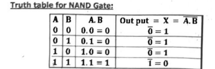
The logic equation for the NAND gate is written $X=\overline{A\cdot B}$ (Read as X equals not A and B). From truth table we can see that the output is low (0) when both inputs A and B are high (1) otherwise output is low (0).
Symbol of NAND Gate:
Truth table for NAND Gate:
| A | B | $A\cdot B$ | Output $=X=\overline{A\cdot B}$ |
|---|---|---|---|
| 0 | 0 | $0\cdot0=0$ | $\overline{0}=1$ |
| 0 | 1 | $0\cdot1=0$ | $\overline{0}=1$ |
| 1 | 0 | $1\cdot0=0$ | $\overline{0}=1$ |
| 1 | 1 | $1\cdot1=1$ | $\overline{1}=0$ |
(v) NOR GATE:
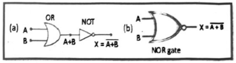
The combination of OR gate with NOT gate is called NOR gate.
A NOR gate is an OR gate with a NOT gate at its output. The symbol for a NOR gate is made from an OR gate with the inversion circle (bubble) at its output as shown in figure below.
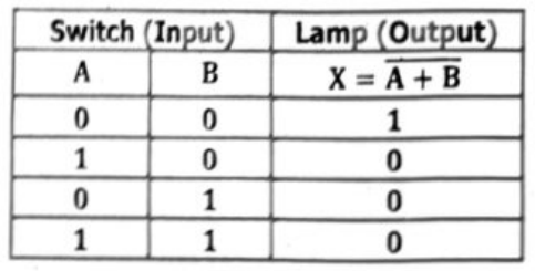
The logic equation for the NOR gate is written as $X = \overline{A + B}$ (Read as X equals not A or B). From truth table we can see that the output is high (1) when both inputs A and B are low (0) otherwise output is high (1).
Symbol of NOR Gate:
Truth table for NOR Gate:
| A | B | A + B | Output = X = $\overline{A + B}$ |
|---|---|---|---|
| 0 | 0 | 0 + 0 = 0 | $\overline{0} = 1$ |
| 0 | 1 | 0 + 1 = 0 | $\overline{0} = 0$ |
| 1 | 0 | 1 + 0 = 0 | $\overline{0} = 0$ |
| 1 | 1 | 1 + 1 = 1 | $\overline{1} = 0$ |
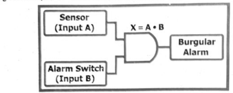
Logic gates are fundamental components in security systems, enabling the creation of circuits that respond to specific conditions to trigger alarms or other protective actions. AND gates are commonly used in burglar alarms to require multiple conditions (like a motion sensor and an open door) to be met before sounding an alarm. OR gates are used in fire alarms to activate when smoke or heat detectors trigger, and also in more complex systems like burglar alarms to combine various sensor inputs.
Examples:
Burglar Alarm:
An AND gate can be used to ensure both a door or window is opened and movement is detected before the alarm is triggered. If only one of these conditions is met, the alarm remains silent.
For example, if the person sensor is ON but the alarm switch is not, the burglar alarm will not be activated. When the person sensor detects the person, it gives the signal 1. Then the alarm switch will also give a signal 1. Thus, “1” and “1” give an output “1” which will make the alarm to ring.
Fire Alarm:
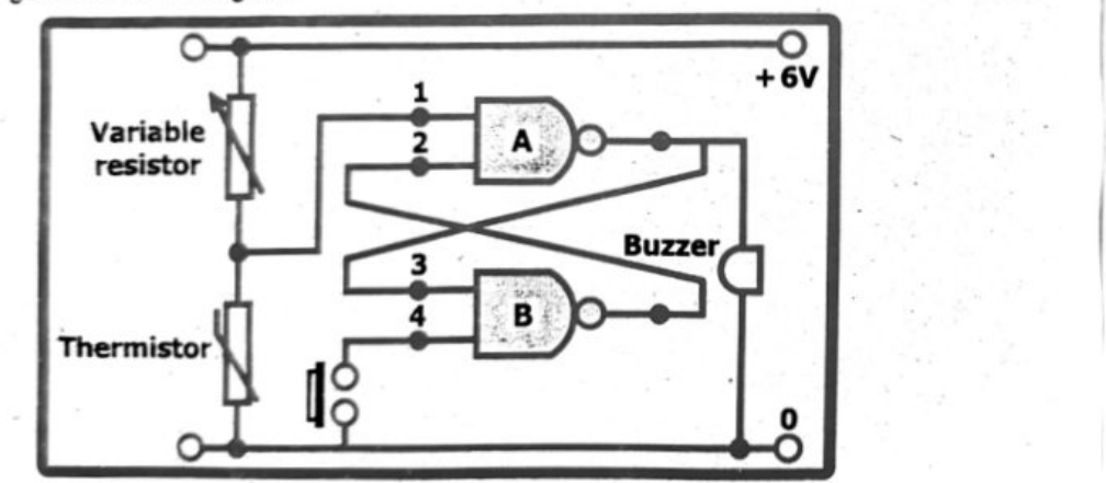
Fire alarm circuit is a simple circuit that detects the fire and activates the Siren Sound. Fire Alarm Circuits are very important devices to detect fire in the right time and prevent any damage to people or property. The circuit is required to switch on when activated then sound a buzzer continuously. A fire alarm circuit using a NAND gate is shown in figure.
The buzzer is initially off so the output from A is 0. This requires the output from gate B must be 1. There being no fire, the thermistor is cold and it's resistance is high, so there is a voltage across it and so the two inputs to gate A are both 1.
When the thermistor is warmed by a fire, it's resistance falls, as does the voltage across it, and input 1 falls to 0. The output from A becomes 1 so there is a voltage across the buzzer, which sounds.
Input 3 to B becomes 1, and since input 4 is also 1, the output from B becomes 0. The inputs to A are 1 and 0, so the output stays at 1. To reset the alarm, the reset switch R must be pressed. This will make input 4 into a 0, so the output from B will be 1 and A will have inputs of 1 and 1, so output 0 as originally.
Following are the circuit symbols for the logic gates:
- AND Gate: $X=A\cdot B$.
- OR Gate: $X=A+B$.
- NOT Gate: $X=\overline{A}$.
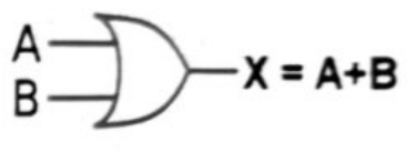
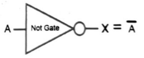
UNIVERSAL LOGIC GATES:
The logic gates NAND and NOR gates are known as “universal gates” because they can be used to make all the other gates.
Working of Universal logic gates NAND and NOR:
NAND GATE:
NAND gate is obtained by coupling a NOT gate with the output terminal of the AND gate, as shown in figure. The NOT gate inverts the output of the AND gate. Symbol of NAND gate is shown in figure (small circle shows the NOT operation). Boolean expression for NAND operation is:
$X=\overline{A\cdot B}$ (read as “X equals A AND B NOT”).
Truth table of NAND Gate:
Switch (Input) Lamp (Output) A B $X=\overline{A\cdot B}$ 0 0 1 1 0 1 0 1 1 1 1 0 NOR GATE:
The NOR gate is obtained by coupling the output of the OR gate with the NOT gate. The NOT gate inverts the output of the OR gate. Boolean expression for NOR operation is:
$X=\overline{A+B}$ (read as “X equals A OR B NOT”).
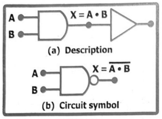
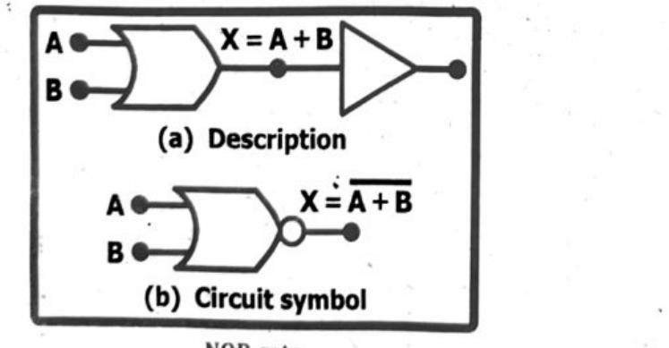
Truth table of NOR Gate:
| Switch (Input) | Lamp (Output) | |
|---|---|---|
| A | B | $X=\overline{A+B}$ |
| 0 | 0 | 1 |
| 1 | 0 | 0 |
| 0 | 1 | 0 |
| 1 | 1 | 0 |
Boolean switches, like transistors, can be combined using logical operations (AND, OR, NOT) to create complex circuits that perform computations. These combinations, called logic gates, are the building blocks of digital circuits and computers. By connecting gates in specific ways, we can build circuits that perform arithmetic, store data, and execute instructions.
Here’s how it works:
Basic Logic Gates:
AND gate: Outputs a 1 only if all inputs are 1.
OR gate: Outputs a 1 if at least one input is 1.
NOT gate: Inverts the input (0 becomes 1, and 1 becomes 0).
Other gates: NAND, NOR, XOR, XNOR, etc., are derived from combinations of the basic three.
Combining Gates:
Series: Connecting gates in series (one after another) implements the AND operation.
Parallel: Connecting gates in parallel implements the OR operation.
Cascading: Combining multiple gates in a sequence allows for complex logic functions.
Examples:
An AND gate followed by a NOT gate creates a NAND gate.
Two AND gates with their outputs ORed together create a more complex logic function.
These circuits can be used to implement any Boolean function.
Building Larger Circuits:
By combining these basic gates, we can construct more complex circuits like:
Adders: Circuits that perform binary addition.
Registers: Circuits that store data.
Multiplexers: Circuits that select one of several inputs based on a control signal.
ALUs (Arithmetic Logic Units): Circuits that perform arithmetic and logical operations within a computer.
In essence, Boolean algebra provides a mathematical framework for designing and understanding these circuits. The ability to translate logical expressions into physical circuits using switches and gates is fundamental to the design of all digital systems.
An NPN bipolar transistor can act as a switch by controlling the flow of current between its collector and emitter terminals based on the current applied to its base terminal. When a sufficient current is applied to the base, the transistor “turns on”, allowing current to flow between the collector and emitter. When the base current is reduced or removed, the transistor “turns off”, blocking current flow. This switching action is achieved by operating the transistor in the saturation (fully on) and cut-off (fully off) regions of its characteristic curves.
Detailed explanation:
Cut-off Region (Off State): When the base current is very low (ideally zero), the transistor is in the cut-off region. In this state, it acts like an open switch, and very little current flows between the collector and emitter.
Saturation Region (On State): When a sufficient base current is applied, the transistor enters the saturation region, acting like a closed switch. In this state, a relatively large current can flow from the collector to the emitter, limited primarily by the load resistance.
Switching Action: By varying the base current, the transistor can be switched between its off and on states, effectively controlling the flow of current in a circuit. For example, a small voltage applied to the base of an NPN transistor can switch on a larger current flowing through a load connected to the collector and emitter, like a lamp or motor.
Transistors:
A transistor is a device composed of semi-conductor material that can both conduct and insulate (e.g. germanium and silicon). Transistors switch and modulate electronic current. The transistor was the first device designed to act as both a transmitter, converting sound waves into electronic waves, and resistor, controlling electronic current. The name transistor comes from the ‘trans’ of transmitter and ‘sistor’ of resistor. These words describe the operation of a transistor which is the transfer of an input signal from a low resistance circuit to a high resistance circuit.
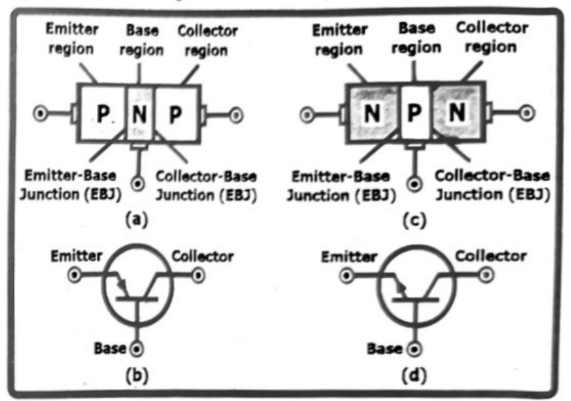
Notation and symbols used with PNP transistor and NPN transistor
In general, all transistors have three regions: base (B), collector (C), and emitter (E).
- Emitter: It is moderately sized and heavily doped region.
- Base: It is at the center of the transistor. It is thin and lightly doped.
- Collector: It is larger than the emitter and is moderately doped.
A transistor is a three-terminal semiconductor device that consists of two p-n junctions namely BE and CE. A transistor is constructed in such a way that a lightly doped region called base is sandwiched between two regions called the emitter and collector. The function of a transistor is to amplify current. This makes them useful as switches or amplifiers. They have an extensive use in electronic devices like televisions, radio transmitters and mobile phones.
TYPES OF TRANSISTOR:
Transistors are made in two types: PNP and NPN.
NPN Transistor:
An NPN transistor is made by joining one P-type semiconductor in between two N-type semiconductors. Here a lightly doped P-type semiconductor is sandwiched between two heavily doped N-type regions.
PNP Transistor:
A PNP transistor is made by sandwiching a N-type semiconductor in between two P-type semiconductors. Here a lightly doped N-type semiconductor is sandwiched between two heavily doped P-type regions.
Transistor is a bi-polar device, bipolar refers to the fact that both holes and electrons participate in the conduction process. If only one carrier is employed (electron or hole), it is considered a unipolar device.
A transistor is a semiconductor device that controls the flow of current in an electronic circuit, acting as either an amplifier or a switch. It essentially regulates a larger current flow based on a smaller input current or voltage. This ability to control current makes transistors fundamental components in electronic devices, enabling functions like signal amplification and digital logic operations.
How Transistors Work:
Switching: Transistors can be used to rapidly switch between “on” and “off” states, controlling whether current flows through a circuit. This is achieved by applying a small voltage or current to the control terminal (base) which then regulates a larger current flow between the other two terminals (emitter and collector).
Amplifying: Transistors can also amplify weak electrical signals, increasing their strength while maintaining the signal’s characteristics. A small input signal applied to the control terminal results in a larger output signal.
Basic Structure: Transistors typically have three terminals: the emitter, base, and collector.
Current Control: A small current or voltage applied to the base terminal controls the current flow between the emitter and collector. This control is achieved by utilizing the properties of semiconductor materials and their ability to conduct or resist current flow based on applied voltages.
An npn transistor under normal operation
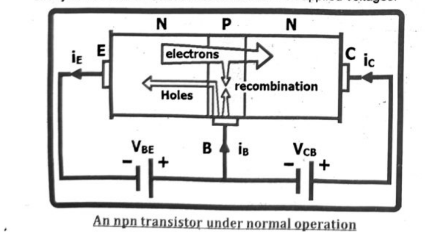
Direction of conventional current in the external circuit is shown in figure. It can be seen that sum of collector current ($I_C$) and base current ($I_B$) is equal to the emitter current ($I_E$), i.e.
$$I_E = I_B + I_C$$
Approximately 95% to 98% of the current through the transistor is from an emitter to collector and about 2% to 5% of the current moves from emitter to base. The ratio between collector current and base current gives the current gain ($\beta$), i.e.
$$\text{Current gain} = \beta = \frac{I_C}{I_B}$$
Equation gives the static or dc value of $\beta$. The dynamic or ac value is calculated for changes in the current values. The ratio between collector current and emitter current gives the current gain ($\alpha$), i.e.
$$\text{Current gain} = \alpha = \frac{I_C}{I_E}$$
Transistors are widely used in digital devices due to their ability to act as both economical and rapid-response switches. Their small size and low cost make them ideal for integrating millions or even billions into a single chip, forming the basis of modern computing and electronics. The rapid switching capabilities of transistors enable them to represent binary data (0s and 1s) and perform complex computations in a very short time, making them essential for processing information in digital devices.
Detailed explanation:
Economical: Transistors are fabricated from materials like silicon, which are abundant and relatively inexpensive. Their small size allows for high integration density, meaning many transistors can be packed onto a single chip, leading to smaller, more powerful, and more affordable devices.
Rapid-Response Switches: Transistors can switch between “on” and “off” states extremely quickly, much faster than mechanical switches. This rapid switching allows them to represent binary data (0 for off, 1 for on) and perform logical operations in digital circuits, forming the basis of everything from simple logic gates to complex processors.
Digital Logic: In digital devices, transistors act as switches in logic gates (AND, OR, NOT, etc.). These gates perform basic logical operations, and when combined, they can create complex circuits that can process information, store data, and execute instructions.
Impact on Modern Technology: The ability to manufacture transistors in large quantities and their switching capabilities have revolutionized electronics, enabling the development of everything from computers and smartphones to medical devices and communication technologies.
Yes, circuits that maintain their state after an input signal is removed can be described as having “memory”. These circuits, often called sequential circuits, are able to store and recall past input values, which influences their current and future outputs. This ability to “remember” past states is what distinguishes them from combinational circuits, where the output is solely determined by the current input.
Detailed explanation:
Sequential Circuits & Memory: Sequential circuits, unlike combinational circuits, have memory elements like flip-flops or latches. These elements store the circuit’s state, which is a representation of past inputs.
How Memory Works: When a sequential circuit receives an input, it can change its state. Importantly, the circuit retains this new state even after the input signal is removed, effectively “remembering” the input.
Examples of Memory Circuits: Flip-flops, registers, and counters are examples of circuits that utilize memory and are fundamental building blocks in digital systems.
Importance of Memory: Memory is crucial for building complex digital systems like computers, where information needs to be stored and processed over time.
Quantum computing is currently in its nascent stage, facing significant manufacturing challenges. A major hurdle is that the core components, qubits, require extremely low temperatures, close to absolute zero, to maintain their quantum state and function properly. This necessitates complex and expensive cooling systems, impacting the scalability and practicality of building larger quantum computers.
Here’s a more detailed explanation:
Qubits and Quantum States:
Quantum computers utilize qubits, which are the quantum mechanical equivalent of classical bits. Unlike classical bits, qubits can exist in a superposition of states (both 0 and 1 simultaneously), enabling them to perform complex computations.
Sensitivity to Environment:
Qubits are extremely sensitive to environmental factors like temperature, vibrations, and electromagnetic interference. These factors can cause “decoherence”, where the qubit loses its quantum state and the computation is corrupted.
Extreme Cooling Requirement:
To minimize decoherence, quantum computers need to be cooled to extremely low temperatures, often near absolute zero. This is achieved using dilution refrigerators, which are complex and expensive pieces of equipment.
Manufacturing and Scalability:
Maintaining superconductivity in qubits and scaling up the number of qubits to build larger quantum computers is a significant manufacturing challenge. Connecting qubits to operate together is also a difficult task as the number of qubits increases.
Error Correction:
Another challenge is the inherent error rate in quantum computations. While quantum computers are theoretically powerful, they are prone to errors, and robust error correction techniques are needed to make them reliable for practical applications.
Hybrid Approach:
While some quantum computing platforms, like superconducting qubits, require extreme cooling, others like photonic qubits can operate at higher, though still cryogenic, temperatures. A hybrid approach, combining different quantum computing platforms, may be necessary for achieving scalability and practicality.
Comparison between analogue and digital signals / electronics:
Analog and digital electronics differ in how they represent and process information. Analog electronics uses continuously variable signals to represent data, while digital electronics uses discrete, binary values (0s and 1s). This fundamental difference leads to variations in their characteristics, applications, and suitability for different tasks.
Detailed comparison:
Analog Electronics:
Signal Representation: Continuous signals with varying voltage and current levels that can represent any value within a range.
Examples: Audio equipment, radio, and certain control systems.
Advantages: Can represent real-world phenomena with high fidelity in some applications.
Disadvantages: Susceptible to noise and interference, making signal degradation more likely. Difficult to store accurately due to the continuous nature of the signal.
Digital Electronics:
Signal Representation: Discrete signals represented by binary values (0s and 1s), making information processing easier.
Examples: Computers, digital communication systems, and modern control systems.
Advantages: Less susceptible to noise and interference, making them more reliable for long-distance transmission. Easy to store and manipulate data due to the binary representation.
Disadvantages: May not capture the nuances of real-world data with the same level of fidelity as analog systems in certain applications. Requires conversion between analog and digital signals for real-world applications.
Digital system has many advantages over analogue, some are given below:
- Digital system has small size.
- Digital systems are generally easier to design.
- Accuracy and precision are greater.
- Digital systems need less power to operate.
- Operation can be programmed.
- Digital circuits are not affected by noise (noise is fluctuations in voltage).
Examples:
When collector current in a junction transistor is 99.9 mA and base current is 0.1 mA, how much is the emitter current?
GIVEN:
- Collector current $I_C$ = 99.9 mA
- Base current $I_B$ = 0.1 mA
REQUIRED:
Emitter current $I_E$ = ?
SOLUTION:
The relationship between emitter, base and collector current is: $I_E = I_B + I_C$
Putting values: $I_E = 99.9\ \text{mA} + 0.1\ \text{mA}$
Therefore, $I_E = 100\ \text{mA}$ or $0.1\ \text{A}$
Emitter current will be 0.1 A.
Find the value of base current required to turn on the transistor for a collector current of 150 mA, for a transistor having current gain $\beta = 190$.
GIVEN:
- Collector current $I_C$ = 150 mA
- Current gain $\beta$ = 190
REQUIRED:
Base current $I_B$ = ?
SOLUTION:
The relationship for current gain is: $\beta = \frac{I_C}{I_B}$ or $I_B = \frac{I_C}{\beta}$
Putting values: $I_B = \frac{150\ \text{mA}}{190}$
Therefore, $I_B = 0.789\ \text{mA}$
Base current to run transistor will be around 0.8 mA.
SUMMARY
- Electronics is the branch of physics that helps to study the emission and behaviour of electrons with electronic devices is known as electronics.
- Semiconductors are materials whose electrical conductivity falls between those of conductors and insulators.
- Intrinsic Semiconductors are pure semiconductors (such as Si or Ge).
- Extrinsic Semiconductors are those semiconductors that are doped with some specific impurities.
- Pentavalent impurities such as phosphorus, arsenic, antimony, and bismuth have five valance electrons and belong to group V–A of periodic table.
- Trivalent impurities e.g., boron, aluminum, indium, and gallium have three valance electrons and belongs to group III–A of periodic table.
- Majority Charge Carriers in n-type semiconductor are electrons and in p-type semiconductor are holes.
- Forward Bias is the condition when the positive terminal of a DC source is connected to p-type and negative terminal is connected to n-type semiconductor of a pn junction.
- Light-Emitting Diode emits energy in the form light when the electric current passes through it.
- Transistor acts as both a transmitter and resistor. It is made in two types: PNP and NPN.
- Relay is an electrically operated switch that open and close the circuits by receiving electrical signals from outside sources.
- Analogue-to-Digital Converter is electronic circuit which can convert the continuously changing analogue signals to discrete digital signals.
- Digital-to-Analogue Converter (DAC) allow to convert discrete digital signal to analogue signals.
- Bit is each digit in binary (0 or 1), which is an abbreviation of binary digit.
- Logic gates implement binary operations to digital electronic circuits.
- Fundamental logic gates are three logic gates AND, OR and NOT logic gates.
- Universal logic gates are the logic gates NAND and NOR because they can be used to make all the other gates.
- Quantum Computing uses phenomena in quantum physics to create new ways of computing.