

Constructed Response Questions:
Consider the given logic circuit:
a) Identify the logic gates in the circuit:
Name of the gate 1 is ____________________
Name of the gate 2 is ____________________
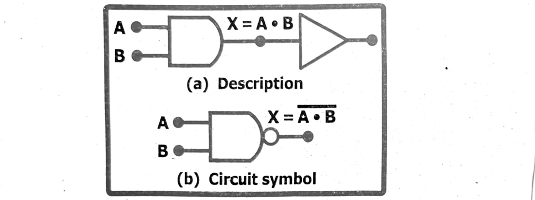
b) Draw a single logic gate that can replace the given logic circuit.
Ans:
a) Identify the logic gates in the circuit:
- Name of the gate 1 is: AND gate
- Name of the gate 2 is: NOT gate
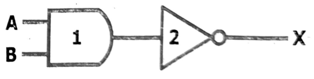
The given logic circuit consists of an AND gate followed by a NOT gate. This combination is known as a NAND gate. Therefore, a single gate can replace the given logic circuit.
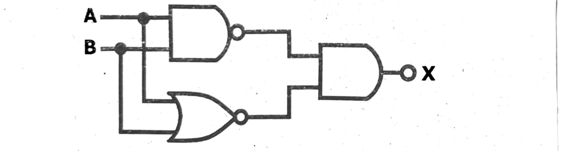
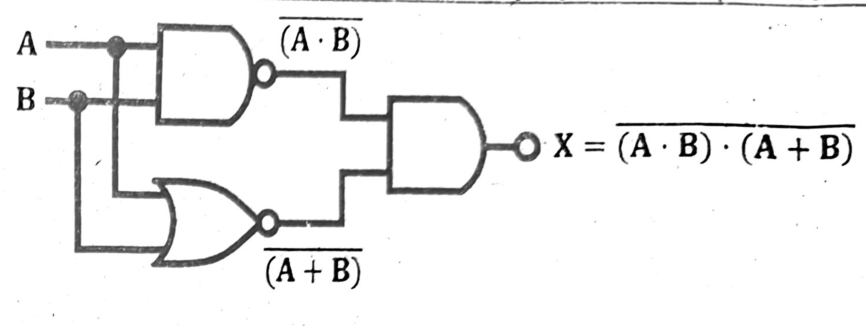
Ans: The circuit consists of an AND gate and an OR gate, followed by a NAND gate.
(i) AND gate:
The output of the AND gate with inputs A and B is $A\cdot B$.
(ii) OR gate:
The output of the OR gate with inputs A and B is $A+B$.
(iii) NAND gate:
The inputs to the NAND gate are the outputs of the AND gate $(A\cdot B)$ and the OR gate $(A+B)$.
So, the expression for the output X is:
$$X=\overline{\overline{(A\cdot B)}\cdot\overline{(A+B)}}=(A\cdot B)+(A+B)$$
TRUTH TABLE:
| Inputs | Output | |||||
|---|---|---|---|---|---|---|
| A | B | $A\cdot B$ | $\overline{(A\cdot B)}$ | $A+B$ | $\overline{(A+B)}$ | $X=\overline{\overline{(A\cdot B)}\cdot\overline{(A+B)}}$ |
| 0 | 0 | 0 | 1 | 0 | 1 | 1 |
| 1 | 0 | 0 | 1 | 1 | 0 | 0 |
| 0 | 1 | 0 | 1 | 1 | 0 | 0 |
| 1 | 1 | 1 | 0 | 1 | 0 | 0 |
Short Questions:
SHORT RESPONSE QUESTIONS
QIII. Give a short response to the following questions.
Ans: In semiconductor devices, N-type materials (doped with impurities that provide extra free electrons) and forward biasing (applying a voltage to encourage current flow) work together to enable electrical conduction.
When a semiconductor device with an N-type region is forward-biased, the potential barrier at the junction is reduced, allowing a significant flow of current, primarily due to the movement of majority carriers (electrons) from the N-type material into the P-type material.
Detailed Explanation:
(i) N-type Material:
- Doping: N-type semiconductors are created by doping a semiconductor material (like silicon) with impurities that have more valence electrons than the semiconductor itself (e.g., phosphorus or arsenic in silicon).
- Majority Carriers: This doping process introduces extra free electrons into the material, making electrons the majority charge carriers.
- Conductivity: The presence of these free electrons enhances the material’s electrical conductivity.
(ii) Forward Biasing:
- Voltage Application: Forward biasing involves connecting the positive terminal of a voltage source to the P-type material and the negative terminal to the N-type material of a semiconductor device, such as a diode.
- Depletion Region Reduction: This voltage reduces the width of the depletion region, which is the area near the junction where there are few free charge carriers.
- Current Flow: The reduced potential barrier allows majority carriers (electrons in the N-type material and holes in the P-type material) to cross the junction and combine, resulting in a significant flow of current.
- Reduced Resistance: As the forward bias voltage increases, the current flow increases, and the resistance of the device decreases, leading to a higher conductivity.
In essence, the N-type material provides the free electrons (majority carriers) that are essential for current flow, and forward biasing provides the necessary voltage to facilitate this flow by reducing the potential barrier at the junction.
Ans: Pentavalent impurities are called donor impurities because they have five valence electrons and when added to a semiconductor, they donate one electron to the crystal, increasing the number of free electrons and thus the conductivity. Conversely, trivalent impurities are called acceptor impurities because they have three valence electrons and when added to a semiconductor, they accept an electron from a neighboring atom to complete their valence shell, creating a “hole” (absence of an electron) which also increases conductivity.
Detailed Explanation:
(i) Pentavalent Impurities (Donors):
- Pentavalent impurities, like phosphorus or arsenic, have five valence electrons.
- When added to a semiconductor like silicon (which has four valence electrons), they create an extra electron that is not needed for bonding.
- This extra electron becomes a free charge carrier and is easily donated to the conduction band, increasing the semiconductor’s conductivity.
- Because they donate an electron, they are called donor impurities.
(ii) Trivalent Impurities (Acceptors):
- Trivalent impurities, like boron or aluminum, have three valence electrons.
- When added to a semiconductor, they create a “hole” (missing electron) in the valence band as they need one more electron to complete their valence shell.
- This hole acts as a positive charge carrier and can move through the semiconductor lattice as electrons move to fill the hole, increasing conductivity.
- Because they accept an electron, they are called acceptor impurities.
In essence, the terms “donor” and “acceptor” describe the behavior of these impurities in relation to electron transfer within the semiconductor crystal, which directly impacts the material’s electrical properties.
Ans: Relays improve electrical systems by enabling the control of high-power circuits with low-power signals, providing isolation between control and load circuits, and automating switching operations. They enhance safety by protecting against faults and overloads, and offer flexibility in circuit design and control.
Detailed look:
(i) Controlling High-Power Loads with Low-Power Signals:
- Relays act as a bridge between low-power control circuits (like those from microcontrollers or sensors) and high-power loads (like motors or industrial machinery).
- A small control signal can activate the relay, which then switches the high-power circuit on or off, preventing direct connection and potential damage to the control components.
- This allows for the automation of complex tasks and efficient operation of large systems with minimal control input.
(ii) Electrical Isolation:
- Relays create a physical and electrical separation between the control circuit and the load circuit.
- This isolation protects sensitive control components from high voltages and currents, reducing the risk of damage and enhancing overall system safety.
(iii) Automated Switching:
- Relays can be programmed or designed to switch circuits based on predefined conditions or timing.
- This automation improves efficiency and reduces the need for manual intervention, particularly in complex systems.
(iv) Safety and Protection:
- Relays are used in safety systems to detect faults (like overloads or short circuits) and automatically disconnect the affected circuit, preventing further damage or hazards.
- Safety relays are crucial in industrial settings to ensure equipment operates within safe parameters.
(v) Flexibility and Customization:
- Relays can be combined in various configurations to create complex switching sequences and control multiple circuits simultaneously.
- This flexibility allows for customized system designs and adaptations to changing operational requirements.
Examples of Relays in Action
- Industrial Automation: A PLC (Programmable Logic Controller) uses a relay to control a large motor, preventing direct connection between the PLC and the motor.
- Home Automation: Relays can control lighting, heating, and other appliances based on time schedules or occupancy sensors.
- Automotive Systems: Power relays manage various functions like headlights, starter motors, and windshield wipers.
- Power Systems: Relays protect power grids and substations from faults and overloads.
- Computer Interfaces: Relays can interface with sensitive electronic equipment and protect them from voltage surges.
Ans: A transistor’s three terminals (base, emitter, and collector) work together to amplify signals by controlling the flow of current between the emitter and collector based on a small current or voltage applied to the base. This amplification occurs because a small change in base current results in a much larger change in collector current.
Detailed Explanation:
- Base: The base terminal acts as a control input. A small current or voltage applied to the base controls the flow of a much larger current between the emitter and collector.
- Emitter: The emitter is the source of charge carriers (electrons or holes, depending on the transistor type).
- Collector: The collector is where the amplified current is collected.
How it works:
- Forward Bias: When a small voltage is applied to the base-emitter junction, it's forward-biased, allowing a small current to flow into the base.
- Current Control: This small base current controls the larger current flowing between the emitter and collector.
- Amplification: The transistor essentially acts as a current-controlled switch, where a small change in base current causes a large change in the collector current.
- Signal Amplification: By carefully selecting the transistor’s operating conditions (biasing) and the external circuit components, the transistor can amplify both current and voltage signals. In simpler terms: Imagine the base as a valve controlling the flow of water (current) from the emitter to the collector. A small turn of the valve (base current) can significantly increase or decrease the water flow (collector current). This principle is how transistors amplify signals, allowing them to be used in various electronic applications, from audio amplifiers to digital logic circuits.
Ans: In a bipolar junction transistor, the emitter is heavily doped to inject a large number of charge carriers, while the base is lightly doped and thin to minimize recombination of these carriers as they pass through it. The collector is moderately doped and larger than the base to effectively collect the charge carriers from the base.
Detailed Explanation:
- Emitter: The emitter is heavily doped to increase the concentration of majority charge carriers (electrons in NPN transistors, holes in PNP transistors). This ensures that a large number of carriers are available to be injected into the base region when the emitter-base junction is forward-biased.
- Base: The base is lightly doped to minimize recombination of charge carriers as they travel from the emitter to the collector. A thin base region further reduces the chances of recombination, allowing most of the injected carriers to reach the collector.
- Collector: The collector is moderately doped and larger than the base. Its primary function is to collect the charge carriers that have passed through the base. The larger size helps to efficiently collect the carriers, while the moderate doping level helps to minimize resistance and prevent the collector from becoming a source of unwanted charge injection.
Essentially, the doping levels and sizes of the different regions are optimized to ensure efficient transistor operation, with the emitter injecting carriers, the base facilitating their transfer, and the collector collecting them.
Ans: In a transistor symbol, the arrow indicates the direction of conventional current flow (the flow of positive charge) through the emitter-base junction. This direction is crucial for understanding how the transistor behaves in a circuit and is a key factor in determining whether it’s an NPN or PNP transistor.
Detailed Explanation:
- NPN Transistors: In NPN transistors, the arrow points outward from the emitter terminal, indicating that conventional current flows out of the emitter.
- PNP Transistors: In PNP transistors, the arrow points inward towards the emitter terminal, indicating that conventional current flows into the emitter.
Why is it important?
- Polarity: The arrow’s direction determines the transistor’s polarity (NPN or PNP).
- Biasing: The arrow helps determine the correct biasing (voltage) required to turn the transistor ON or OFF.
- Circuit Analysis: Understanding the arrow’s direction is essential for analyzing and designing transistor circuits.
- Current Flow: The arrow indicates the direction of conventional current flow, which is the direction of positive charge movement.
Ans: Normal biasing of an NPN transistor involves applying voltage in a way that forward biases the base-emitter junction and reverse biases the base-collector junction. This configuration allows the transistor to act as an amplifier or switch, controlling a larger current with a smaller input signal.
Here’s a more detailed explanation:
Forward Biasing the Base-Emitter Junction:
- A positive voltage is applied to the base relative to the emitter.
- This creates a flow of electrons from the emitter (n-type) into the base (p-type).
- The base is lightly doped and thin, so most of these electrons don’t recombine with holes in the base, and instead, they are injected into the collector region.
Reverse Biasing the Base-Collector Junction:
- A positive voltage is applied to the collector relative to the base.
- This creates a depletion region at the base-collector junction, preventing a direct flow of current.
- The electrons injected from the emitter into the base are attracted to the positive collector, creating a collector current.
Current Flow:
- The forward-biased base-emitter junction allows a small base current ($I_B$) to flow, which controls a much larger collector current ($I_C$).
- The ratio of $I_C$ to $I_B$ is called the current gain ($\beta$) of the transistor.
- The emitter current ($I_E$) is the sum of the base current and the collector current ($I_E = I_B + I_C$).
In Summary:
By forward biasing the base-emitter junction and reverse biasing the base-collector junction, the NPN transistor allows a small base current to control a much larger collector current, enabling its use in various electronic circuits.
What Happens If the Biasing Is Reversed?
If the biasing is reversed (emitter-base junction reverse-biased and collector-base forward-biased), the transistor doesn’t function properly. Only a very small leakage current flows, and it cannot amplify signals. Essentially, it acts like an open switch or becomes non-conductive, breaking the normal operation of the circuit.
Ans: In a diode, the depletion region changes its width based on whether it’s forward or reverse biased. Forward bias decreases the depletion region’s width, while reverse bias increases it. This change in width affects the diode’s ability to conduct current.
Forward Bias:
- When a diode is forward-biased, the positive terminal of the voltage source is connected to the p-side (anode), and the negative terminal is connected to the n-side (cathode).
- This configuration reduces the electric field across the depletion region and causes it to narrow.
- The applied voltage pushes electrons from the n-side and holes from the p-side towards the junction, effectively reducing the barrier to current flow.
- When the forward voltage overcomes the barrier potential (approximately 0.7 V for silicon diodes), the depletion region narrows significantly, allowing a large current to flow.
Reverse Bias:
- In reverse bias, the positive terminal of the voltage source is connected to the n-side (cathode), and the negative terminal is connected to the p-side (anode).
- This configuration increases the electric field across the depletion region and causes it to widen.
- The applied voltage pulls electrons away from the junction on the n-side and holes away from the junction on the p-side, increasing the depletion region’s width.
- This widening creates a larger barrier for current flow, and only a small reverse saturation current due to minority carriers flows.
In essence, forward bias encourages current flow by narrowing the depletion region, while reverse bias hinders current flow by widening it.
Forward bias = narrow depletion region = current flows
Reverse bias = wide depletion region = little to no current
Ans: Despite the presence of majority charge carriers (free electrons in n-type and holes in p-type), n-type and p-type semiconductor materials are electrically neutral because the charge of these carriers is balanced by the charge of the dopant atoms. While n-type materials have excess free electrons, the donor atoms that provided those electrons are left with a positive charge. Similarly, p-type materials have an excess of holes, but the acceptor atoms that created these holes have a negative charge.
Detailed explanation:
(i) N-type semiconductors:
- Doping: N-type semiconductors are created by doping a semiconductor (like silicon) with a small amount of a pentavalent element (like phosphorus or arsenic).
- Free electrons: The dopant atoms have five valence electrons, but only four are needed to form covalent bonds with the silicon atoms. The extra electron becomes a free electron, contributing to the electrical conductivity.
- Positive dopant ions: When a pentavalent atom donates an electron, it becomes a positively charged ion. However, the number of positive ions is equal to the number of free electrons, resulting in a net charge of zero for the material.
(ii) P-type semiconductors:
- Doping: P-type semiconductors are created by doping a semiconductor with a trivalent element (like boron or gallium).
- Holes: Trivalent atoms have only three valence electrons. When these atoms bond with silicon, they create a “hole” where an electron is missing. This hole acts like a positive charge carrier as electrons can move into the hole.
- Negative dopant ions: When a trivalent atom accepts an electron to fill the hole, it becomes a negatively charged ion. The number of negatively charged ions is equal to the number of holes, maintaining electrical neutrality.
Overall:
- In both n-type and p-type materials, the movement of charge carriers (electrons or holes) is balanced by the stationary charge of the dopant atoms, resulting in a net charge of zero for the material.
- The “n” and “p” designations refer to the type of majority charge carriers (negative for n-type, positive for p-type), not the overall charge of the material.
Ans: NAND and NOR gates are called universal gates because they can be used to implement any other logic gate or Boolean function. This means that with only NAND gates or only NOR gates, you can create circuits that perform the functions of AND, OR, NOT, XOR, and other logic gates.
- NAND as a Universal Gate: A NAND gate (Not AND) combines the functions of an AND gate and a NOT gate. By strategically connecting NAND gates, you can create NOT, AND, OR, XOR, and other logic gates.
- NOR as a Universal Gate: Similarly, a NOR gate (Not OR) combines the functions of an OR gate and a NOT gate. Like NAND gates, NOR gates can be combined to form any other logic gate.
- Functionally Complete: Because NAND and NOR gates can create any other logic function, they are considered “functionally complete” or “universal”.
- Practical Implications: This universality makes NAND and NOR gates very useful in digital circuit design because they can simplify the number of different gate types needed in a circuit.
Essentially, you can build any logic circuit you need using only NAND gates or only NOR gates, which is why they are called universal gates.
Ans: A NOR (Not-OR) gate produces a HIGH (1) output only when all its inputs are LOW (0). If any input is HIGH (1), the output will be LOW (0). In essence, it’s the opposite of an OR gate, hence the “Not-OR” name.
For a two-input NOR gate (inputs A and B, output X):
$X=\overline{A+B}$
- Inputs: A NOR gate can have multiple inputs (2 or more).
- Output: The output is a single signal.
Truth Table:
- If all inputs are 0, the output is 1.
- If any input is 1, the output is 0.
Example:
- If a two-input NOR gate has inputs A = 0 and B = 0, the output is 1.
- If a two-input NOR gate has inputs A = 1 and B = 0, the output is 0.
- If a two-input NOR gate has inputs A = 0 and B = 1, the output is 0.
- If a two-input NOR gate has inputs A = 1 and B = 1, the output is 0.
Truth table of NOR Gate:
| Switch (Input) | Lamp (Output) | |
|---|---|---|
| A | B | $X=A+B$ |
| 0 | 0 | 1 |
| 1 | 0 | 0 |
| 0 | 1 | 0 |
| 1 | 1 | 0 |
Ans: Digital systems generally offer several advantages over analog systems, primarily due to their ability to represent information as discrete values, making them more robust and versatile. Key benefits include higher accuracy, greater noise immunity, easier storage and transmission, and simpler processing.
Detailed Comparison:
Accuracy and Noise Immunity:
- Digital: Digital systems use discrete values (like 0s and 1s) to represent information. This allows for precise signal regeneration during transmission, minimizing the impact of noise and distortion. Error detection and correction codes can further enhance accuracy by identifying and fixing errors.
- Analog: Analog signals are continuous, making them susceptible to noise and distortion during transmission and processing. Any unwanted signal can easily corrupt the original data.
Storage and Transmission:
- Digital: Digital data can be easily stored on various media like hard drives, flash memory, or optical disks. It can also be compressed and transmitted efficiently, with little to no loss of information.
- Analog: Analog signals are more challenging to store and transmit without degradation. Storing and reproducing analog signals can be complex and lead to signal degradation.
Processing and Flexibility:
- Digital: Digital systems offer greater flexibility in signal processing due to the ability to use algorithms and programmable systems. Complex signal processing tasks like filtering, Fourier transforms, and other algorithms can be implemented and altered with ease.
- Analog: Analog signal processing can be more challenging, especially for complex tasks. Modifying analog circuits to perform different functions can be difficult.
Cost and Scalability:
- Digital: Digital systems, particularly those based on microcontrollers or DSPs, can have higher initial costs for complex applications. However, their scalability and re-programmability often lead to lower long-term costs for complex tasks.
- Analog: Analog systems can be simpler to design for basic functions, but their complexity can increase significantly for more advanced tasks. They may also lack the scalability of digital systems.
Ease of Design and Understanding:
- Digital: Digital circuits are often easier to understand and design due to their abstraction of underlying complex systems. This makes it easier to create and maintain digital systems.
- Analog: Analog circuit design can be more intricate and require specialized knowledge.
In summary, while analog systems have their place, digital systems generally offer superior accuracy, noise immunity, flexibility, and ease of storage and processing. This makes them the preferred choice for most modern applications, particularly those involving complex computations, data storage, and reliable transmission.
Long Questions:
Ans: An extrinsic semiconductor is a semiconductor material with added impurities (dopants) to enhance its electrical conductivity. These impurities alter the number of free charge carriers (electrons or holes) within the semiconductor’s crystal lattice, significantly increasing its ability to conduct electricity compared to an intrinsic (pure) semiconductor.
How Impurities Affect Conductivity:
Doping Process:
Extrinsic semiconductors are created by doping, which involves introducing specific impurities into a pure semiconductor material.
Increased Charge Carriers:
- N-type: When a pentavalent impurity (like phosphorus) is added, it introduces extra free electrons into the semiconductor’s lattice, increasing the number of negative charge carriers (electrons).
- P-type: When a trivalent impurity (like boron) is added, it creates “holes” (vacancies where electrons should be) in the lattice, increasing the number of positive charge carriers (holes).
Enhanced Conductivity:
The increased concentration of charge carriers (either electrons or holes) due to doping significantly enhances the semiconductor’s ability to conduct electricity compared to a pure semiconductor.
Controlled Conductivity:
The type and concentration of dopants can be precisely controlled, allowing for the creation of semiconductors with specific desired electrical properties.
Ans: A PN junction is formed when a p-type semiconductor (excess of holes) and an n-type semiconductor (excess of electrons) are brought into contact. When forward biased, the junction allows current to flow easily, while reverse biasing significantly restricts current flow. This difference in behavior is due to the changes in the depletion region width and the potential barrier.
Formation of a PN Junction:
- Semiconductor Materials: A p-type semiconductor is created by doping a material like silicon with impurities that create “holes” (vacancies for electrons). An n-type semiconductor is created by doping with impurities that create free electrons.
- Contact: When a p-type and n-type material are joined, free electrons from the n-side diffuse to the p-side, and holes from the p-side diffuse to the n-side.
- Depletion Region: This diffusion creates a region near the junction devoid of free charge carriers (electrons and holes), called the depletion region. This region develops a potential barrier due to the charged ions left behind by the diffused carriers.
- Equilibrium: At equilibrium, the diffusion of carriers is balanced by the potential barrier, preventing further diffusion.
Forward Bias:
- Connection: In forward bias, the positive terminal of a voltage source is connected to the p-type material and the negative terminal to the n-type material.
- Depletion Region: The applied voltage reduces the width of the depletion region and lowers the potential barrier.
- Current Flow: This reduction in barrier height allows majority carriers (electrons in n-type and holes in p-type) to easily cross the junction and flow as current.
- Resistance: Forward bias significantly reduces the resistance of the diode, allowing current to flow easily.
Reverse Bias:
- Connection: In reverse bias, the positive terminal of the voltage source is connected to the n-type material and the negative terminal to the p-type material.
- Depletion Region: The applied voltage widens the depletion region and increases the potential barrier.
- Current Flow: The increased barrier restricts the flow of majority carriers. Only a small leakage current due to minority carriers (electrons in p-type and holes in n-type) flows.
- Resistance: Reverse bias increases the resistance of the diode, significantly hindering current flow.
- Breakdown: At a high enough reverse voltage, the diode can undergo breakdown, leading to a large increase in current and potentially damaging the device.
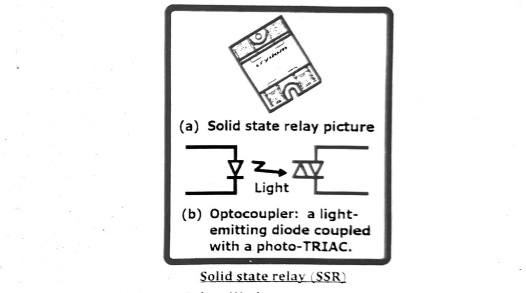
Ans: A solid-state relay (SSR) uses semiconductors to switch electrical circuits, offering advantages like faster switching speeds, longer lifespan, and resistance to wear and tear compared to mechanical relays. A typical SSR uses an optocoupler to isolate input and output circuits, and semiconductor components like TRIACs, thyristors, or MOSFETs to control the load current.
How Solid-State Relays Work:
- Input Signal: A low-power electrical signal (DC or AC) is applied to the input of the SSR.
- Optocoupler Isolation: This signal is typically converted into a light signal, often infrared, by an LED within the optocoupler.
- Output Switching: The light from the LED is detected by a light-sensitive semiconductor, which then controls the output circuit.
- Load Control: The output circuit, often using components like TRIACs or MOSFETs, switches the flow of a larger current to the load.
Advantages of SSRs over Mechanical Relays:
- Faster Switching Speed: SSRs can switch on and off much faster than mechanical relays, which have moving parts.
- Longer Lifespan: Without physical contacts, SSRs are not susceptible to wear and tear, resulting in a longer lifespan and higher reliability.
- No Contact Bounce: SSRs eliminate contact bounce, which is a common issue with mechanical relays that can cause erratic behavior.
- Silent Operation: SSRs operate silently, unlike mechanical relays that make a clicking noise when switching.
- Immunity to Vibration and Noise: SSRs are less susceptible to vibration and electrical noise, making them suitable for harsh environments.
- Lower Power Consumption: In some cases, SSRs consume less power than mechanical relays.
- Smaller Size: SSRs can be smaller than mechanical relays, especially for high-current applications.
In essence, SSRs offer a more robust, faster, and longer-lasting solution for switching electrical loads compared to traditional mechanical relays.
Ans: An NPN transistor operates by controlling the flow of electrons (majority charge carriers) between its emitter and collector terminals, using a small base current. When a small positive voltage (relative to the emitter) is applied to the base, it allows a larger current to flow from the collector to the emitter. This action is due to the movement of electrons, which are attracted from the emitter, through the thin base region, and to the collector.
Detailed Explanation:
- Structure: An NPN transistor consists of a layer of p-type semiconductor (the base) sandwiched between two n-type layers (the emitter and collector).
- Base-Emitter Junction: When a small positive voltage (relative to the emitter) is applied to the base, it forward-biases the base-emitter junction. This causes electrons in the emitter to be injected into the base region.
- Base Region: The base region is thin and lightly doped, meaning it has a small number of holes (minority carriers). Most of the electrons injected from the emitter diffuse through the base.
- Base-Collector Junction: The base-collector junction is reverse-biased, meaning it normally blocks current flow. However, the electrons diffusing through the base are attracted to the positive voltage at the collector, creating a current flow from collector to emitter.
- Amplification: By controlling the base current, the transistor controls the much larger collector current. A small change in the base current can result in a large change in the collector current, making the transistor useful for amplification.
- Switching: When the base current is zero, the transistor is off, and little current flows from collector to emitter. When the base current is sufficient, the transistor switches on, allowing a large current to flow.
Ans: A transistor can act as a switch by controlling the flow of current between its collector and emitter terminals based on the voltage applied to its base terminal. When a sufficient voltage is applied to the base, the transistor “turns on,” allowing current to flow through it, similar to a closed switch. When the base voltage is low, the transistor “turns off,” blocking current flow, like an open switch.
How it works:
- Bipolar Junction Transistors (BJTs): In a BJT, a small current applied to the base terminal controls a much larger current flow between the collector and emitter.
- Field-Effect Transistors (FETs): In FETs, a voltage applied to the gate terminal controls the current flow between the source and drain.
- Switching Action: By varying the voltage at the base (BJT) or gate (FET), the transistor can be switched between an “on” and “off” state, effectively controlling the current flow in the circuit.
Examples of Transistor as a Switch:
- LED Control: A transistor can be used to switch an LED on or off by controlling the current flow through it.
- Motor Control: Transistors can be used to control the on/off state of DC motors, allowing them to be turned on and off with a smaller control signal.
- Relay Control: Transistors can act as drivers for relays, allowing a low-power signal to switch on/off higher voltage or current circuits.
- Logic Gates: Transistors are fundamental building blocks of logic gates (AND, OR, NOT, etc.) in digital circuits, where they act as switches to perform logical operations.
- Power Supplies: Transistors are used in switched-mode power supplies to efficiently regulate voltage and current by rapidly switching between on and off states.
- Amplification: While transistors are also used as amplifiers, the switching behavior is crucial in many amplifier circuits where they switch between states to amplify signals.
In essence, transistors act as electronic switches that enable us to control the flow of electricity in various circuits, from simple LED circuits to complex digital logic and power management systems.
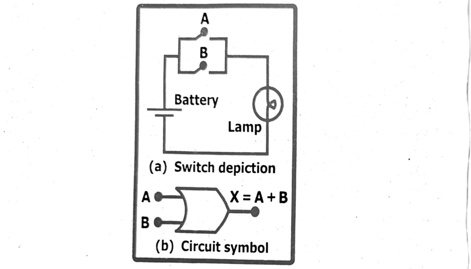
Ans: An OR gate outputs a high signal (1) if at least one of its inputs is high. Otherwise, it outputs a low signal (0). This behavior can be represented with a truth table and visualized with a simple circuit.
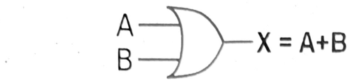
Output of OR gate will be ‘0’ only when all of its inputs are ‘0’, and for all other situations output of OR gate will be ‘1’.
Truth table of OR Gate:
| OR GATE | ||
|---|---|---|
| Switch (Input) | Lamp (Output) | |
| A | B | X = A + B |
| 0 | 0 | 0 |
| 1 | 0 | 1 |
| 0 | 1 | 1 |
| 1 | 1 | 1 |
In essence, the OR gate works by allowing current to flow to the output if any of its inputs are at a high voltage level. This corresponds to the logical OR operation, where the output is true (1) if at least one of the inputs is true (1).
Ans: Logic gates are fundamental components in both burglar alarms and fire extinguishers, enabling them to respond to specific conditions and trigger appropriate actions. In burglar alarms, they process inputs from sensors (like door / window contacts and motion detectors) to determine if an intrusion has occurred, activating the alarm accordingly. For fire extinguishers, logic gates can be used in more advanced systems to monitor environmental factors and automatically activate the extinguisher when a fire is detected.
Burglar Alarms:
Basic Concept:
Burglar alarms use logic gates to create a circuit that is normally “off” (no alarm) unless a specific set of conditions is met. These conditions are typically changes in sensor inputs that indicate a potential intrusion.
Example:
A simple burglar alarm might use an AND gate. The inputs could be:
- Input 1: A switch connected to a door, which is “on” when the door is closed and “off” when the door is open.
- Input 2: A motion detector, which is “on” when motion is detected and “off” otherwise.
- The AND gate output would be “on” (triggering the alarm) only when both inputs are “on” (the door is open AND motion is detected). This prevents false alarms from a door opening without anyone entering.
More Complex Systems:
More sophisticated systems might use combinations of AND, OR, and NOT gates to process inputs from various sensors, creating a layered security system. For instance, a system could use an AND gate for a door sensor and a motion sensor, but also include an OR gate that triggers the alarm if either the door sensor OR a window sensor is triggered. A NOT gate might be used to inhibit the alarm in specific cases, such as during a pre-set disarming period.
Fire Extinguishers:
Basic Concept:
In fire extinguishers, logic gates can be used to process data from various sensors (temperature, smoke, etc.) and activate the extinguisher when a fire is detected.
Example:
A simple fire alarm system might use an OR gate. The inputs could be:
- Input 1: A heat sensor which is “on” when a high temperature is detected.
- Input 2: A smoke detector, which is “on” when smoke is detected.
- The OR gate output would be “on” (activating the extinguisher) if either the heat sensor OR the smoke detector is triggered.
More Complex Systems:
More advanced fire extinguisher systems could incorporate more complex logic using AND, OR, NOT gates and potentially timers to ensure the extinguisher is activated only when a fire is clearly present and to prevent false alarms. For example, a system might use an AND gate with inputs from a smoke detector, a heat sensor, and a timer (to allow for momentary temperature fluctuations) to ensure the extinguisher is activated only after a sustained fire hazard is detected.
In Summary: Logic gates provide the foundation for both burglar alarms and fire extinguishers, allowing them to intelligently respond to environmental changes by processing sensor inputs and activating the appropriate response based on logical operations.
Ans: The development of quantum computers faces numerous technical, practical, and theoretical challenges. These include maintaining stable quantum states (lowering decoherence), scaling the number of qubits, developing effective quantum error correction, and creating robust and scalable quantum hardware. Additionally, the high cost of building and operating quantum computers and the need for specialized talent in quantum physics, engineering, and statistics present significant hurdles.
Detailed Breakdown:
Maintaining Quantum States (Decoherence):
- Challenge: Qubits, the quantum equivalent of classical bits, are highly sensitive to their environment. External factors like temperature fluctuations, electromagnetic fields, and even vibrations can cause a qubit to lose its quantum state (decoherence), leading to errors in computations.
- Impact: Decoherence is a major obstacle in building large-scale, reliable quantum computers.
- Solutions: Scientists are exploring various approaches, including developing new materials and computational techniques to mitigate decoherence.
Scaling Qubits:
- Challenge: Current quantum computers have a limited number of qubits, and scaling them up to the millions needed for practical applications is a major hurdle.
- Impact: The complexity of controlling and interacting with a large number of qubits increases exponentially, making it difficult to design and build large-scale quantum processors.
- Solutions: Researchers are exploring different qubit technologies (superconducting, trapped ions, etc.) and architectures to overcome scalability limitations.
Quantum Error Correction:
- Challenge: Quantum computations are inherently prone to errors due to the factors mentioned above. Error correction is crucial for building fault-tolerant quantum computers.
- Impact: Current error correction methods are resource-intensive, requiring a large number of physical qubits to represent a single logical qubit.
- Solutions: Research is focused on developing more efficient error correction codes and algorithms.
Hardware Development:
- Challenge: Quantum computers require specialized hardware that can operate at extremely low temperatures (near absolute zero) and are highly sensitive to environmental noise.
- Impact: This necessitates advanced and costly cryogenic systems, limiting the scalability and accessibility of quantum computers.
- Solutions: Researchers are exploring different qubit technologies and materials to reduce the need for extreme cooling and improve hardware robustness.
Algorithmic Development:
- Challenge: Quantum algorithms are fundamentally different from classical algorithms, requiring new programming paradigms and specialized tools.
- Impact: There is a shortage of quantum software engineers and a lack of established programming frameworks.
- Solutions: Efforts are underway to develop quantum programming languages, compilers, and libraries.
Cost and Accessibility:
- Challenge: Building and maintaining quantum computers is extremely expensive, with the cost per qubit currently estimated at $10.000.
- Impact: High costs limit the widespread adoption of quantum computing and restrict access to research and development efforts.
- Solutions: Reducing the cost of qubit fabrication, hardware components, and operating quantum systems is crucial.
Talent Shortage:
- Challenge: There is a significant shortage of qualified quantum researchers and engineers with the necessary expertise in quantum physics, engineering, and computer science.
- Impact: This limits the pace of research and development in the field.
- Solutions: Investing in education and training programs to build a larger pool of quantum experts is crucial.
Environmental Concerns:
- Challenge: The energy consumption and cooling requirements of quantum computers can raise environmental concerns, particularly for large-scale systems.
- Impact: This could hinder the adoption of quantum computing in environmentally conscious industries.
- Solutions: Developing more energy-efficient quantum hardware and exploring alternative cooling methods are important.
In conclusion, while quantum computing holds immense promise for revolutionizing various fields, it faces a multitude of technical and practical challenges that require sustained research, development, and collaboration across multiple disciplines.